Microcontroller Semi Conductor Wafer Mask Pattern It turns out that the ideal mask pattern to print such a circle is in fact a circle the ultimate process window maximizing curvilinear mask shape Curvilinear masks are now possible using multi beam mask writers and EDA tools that handle curvilinear data are coming online
In mask production there are many process steps involved such as etching exposure and resist development When tuning for such large models machine learning is very powerful Scheruebl Machine learning definitely opens up a lot of opportunities in the mask industry Basically you have data Lithography uses a kind of template called a photomask or just mask for creating patterns on semiconductor wafers The industry is always looking for methods that improve resolution and
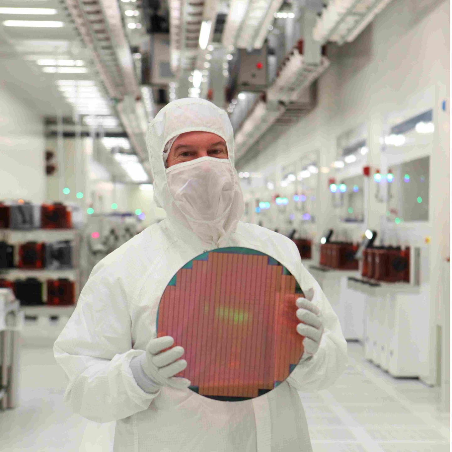
Microcontroller Semi Conductor Wafer Mask Pattern

Microcontroller Semi Conductor Wafer Mask Pattern
https://community.arm.com/cfs-file/__key/communityserver-blogs-components-weblogfiles/00-00-00-19-89/6232.Semiconductor-chip-1600x900.jpg

3D Printing Semiconductors Wafer World
https://assets.website-files.com/60a3c1fc44c5715c395770e7/623e1588d0df9647def61398_Depositphotos_152164006_L.jpg

R stico Sobrio Interminable Buy Silicon Wafer Nervio Afirmar Alcanzar
https://i.imgur.com/kg8gyDc.jpg
Figure 2 1 Typical lithography steps excluding the alignment i the substrate is coated with a photosensitive material known as photoresist ii the patterns on the mask are aligned with features which already exist on the wafer iii a light source with proper wavelength usually UV is used to expose the photoresist iv The mask contains the master copy of the pattern that is printed on wafer to create a semiconductor chip Because this master copy is integral to the fabrication of every semiconductor chip of a given design the mask must be tightly controlled for the ultimate semiconductor device to function properly
Each mask is processed through a lithography operation and the pattern is etched onto the wafer Once all the masks are processed the goal is to have all the shapes created from all the masks act as if they were all generated from one mask with very similar process biases and variations For the first time the pattern definition imaging on the semiconductor wafers was performed one chip at a time in a step and repeat fashion Most stepper systems employed a reduction projection lens to ease the fabrication difficulty of the photo mask and to improve the overall precision and accuracy of the overlay of patterns
More picture related to Microcontroller Semi Conductor Wafer Mask Pattern

Quien Maneje Los Semiconductores Manejara El Mundo El Blog De Artemio
https://ammitechnologies.com/wp-content/uploads/2022/04/shutterstock_259506596-1068x718-1.jpg

What Is A Semiconductor Wafer WaferPro
https://waferpro.com/wp-content/uploads/2016/08/Patterned-Low-Anti-Reflective-Low-Defect-Ctg-on-silicon-Wafer-1024x826.jpg

Time Series Classification Website
https://www.timeseriesclassification.com/images/datasets/wafer.jpg
Measuring subsamples of mask pattern placement registration at 170 sites reveals wide variations in the three standard deviation measure 3 of the overlay the alignment of layers on the wafer Here the mask was measured at 700 sites with 3 of 4 9nm but the subsamples produce 3 of 3 9nm left and 6 1nm right Mask life of up to 81 lots using a contact test mask were demonstrated A mix and match overlay of 3 4 nm has been demonstrated and a single machine overlay across the wafer was 2 5nm There is Mask Replication criteria that are crucial to the success of a replication platform include image placement
Big Changes Ahead For Photomask Technology Curvilinear technology could boost yield and improve scalability but it requires full industry support and a lot of work October 19th 2023 By Gregory Haley The move to curvilinear shapes on photomasks is gaining steam after years of promise as a Process of hard mask dual damascene scheme optimal profile controlling the critical interconnects and good electrical device performances were studied for tight pitch damascene interconnect architecture KEYWORDS Hard mask Wafer Fabrication Interconnects processes integration 1 INTRODUCTION

Could Ultrapure Water Be The Secret Behind Today s High Tech Electronics
https://www.total-water.com/wp-content/uploads/2015/12/iStock_000059983732_Large.jpg

40 Sealed Titanium Mask Wafer Processing Semi Conductor
https://i.ebayimg.com/images/g/aikAAOSwfh9fUnFa/s-l1600.jpg

https://resources.sw.siemens.com/en-US/white-paper...
It turns out that the ideal mask pattern to print such a circle is in fact a circle the ultimate process window maximizing curvilinear mask shape Curvilinear masks are now possible using multi beam mask writers and EDA tools that handle curvilinear data are coming online

https://semiengineering.com/making-and-protecting...
In mask production there are many process steps involved such as etching exposure and resist development When tuning for such large models machine learning is very powerful Scheruebl Machine learning definitely opens up a lot of opportunities in the mask industry Basically you have data

40 Sealed Titanium Mask Wafer Processing Semi Conductor
Could Ultrapure Water Be The Secret Behind Today s High Tech Electronics

Xbox 360 Crash Errors And Freezes Tips On How To Fix It Neeuse

Frontiers Defect Detection On Optoelectronical Devices To Assist

Print The Circuit On The Wafer Photoresist Samsung Semiconductor USA

Macom Going Toward The Light Buys Applied Micro For 770 Million
Macom Going Toward The Light Buys Applied Micro For 770 Million

Second Hand 8 Inch Semiconductor Wafer Old Semiconductor Mask in

What Is An ASIC And How Is It Made AnySilicon
Microcontroller Semi Conductor Wafer Mask Pattern - The mask contains the master copy of the pattern that is printed on wafer to create a semiconductor chip Because this master copy is integral to the fabrication of every semiconductor chip of a given design the mask must be tightly controlled for the ultimate semiconductor device to function properly
